


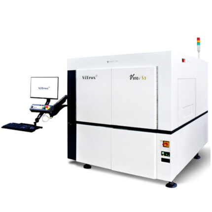

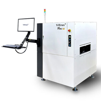
V310i SE ViTrox | 3D Advanced Optical Inspection (SPI)
V310i SE ViTrox (SPI)
- Preferred choice by consumer, automotive, and telecommunication sectors.
- Powerful reporting for data analysis and performance monitoring.
- High Speed performance SPI system in market.
- Smart Manufacturing Ready
3D Advanced Optical
Advanced Process Optimization
Collaborate with market known printer and pick & place partners. ViTrox AI profiles out the best printer settings for each production model. This is achieved through continuous data collection on printer optimization activities.
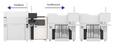
Interconnection between Printer, SPI & SMT
Unique Inspection Coverage
Cater to various inspection coverages within a modified machine platform including gold finger, distance measurement, gold pads, red glue by using ViTrox generic programming platform.
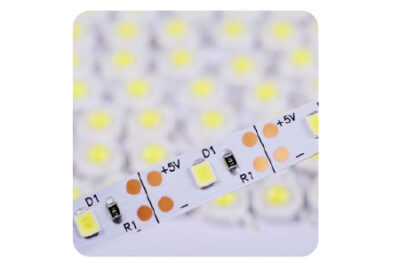
LED
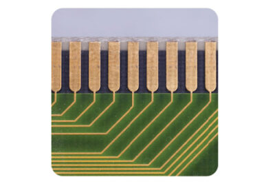
Gold Finger
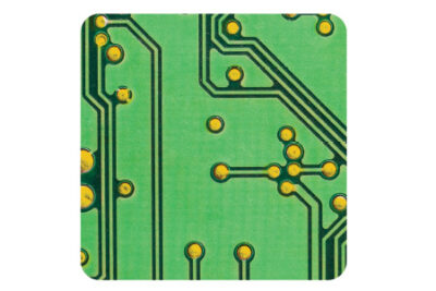
Red Glue
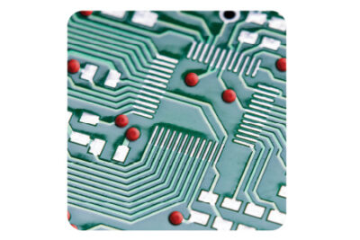
Gold Pads
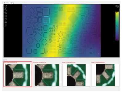
Powerful PCB Analysis
Analyze board warpages and prevent it from flowing through to the next process to achieve optimum quality with no rework cost.
| Model.No | V310i SE | |
| Inspection Functions | Missing, XY Offset, Solder Height, Solder Area, Solder Volume and Bridge. | |
| Board Level Tracebility | Camera-Read Barcodes; External Barcode Reader Configured | |
| System Hardware | 12 MP 4 MP | |
| Operating System | Windows 10 Pro (64 bit) | |
| Optical Resolution & FOV Size | Default: 60mmx45mm @ 15µm telecentric lens Option: 53mmx39mm @ 13µm telecentric lens Option: 32mmx24mm @ 8µm telecentric lens |
Default: 40mmx40mm @ 20µm telecentric lens |
| Inspection Speed | 12MP CoaXPress @ 15µm Resolution: Up to 94cm²/sec
12MP CameraLink @ 15µm Resolution: Up to 60cm²/sec |
4MP CameraLink: 40~53cm²/sec |
| 3D Technologies | Phase Shift Profilometry’s (PSP) Methodology | |
| Lighting Module | Concurrent Lighting Module | |
| Conveyor Width Adjustment | Auto Width Adjustment; Bottom-Up Clamping; In-line SMEMA | |
| Installation Specification | ||
| Power Supplies | 100-120 V, 16A/200-240V, 8A Single Phase | |
| Air requirement | N/A | |
| System footprint (Width X Depth X Height) | 1060mmx1303mmx2000mm | |
| Total system weight | ~830kgs | |
| PCB Dimension | SE | FDL |
| Maximum PCB Size (L x W) | 510mmx540mm (20”x21.2”) | Single Lane: 510mmx450mm (20”x17.7”) DL Equal: 510mmx250mm (20”x9.8”) |
| Minimum PCB Size (L x W) | 50mmx50mm (2”x2”) | 50mmx50mm (2”x2”) |
| Maximum PCB Inspectable Area (L x W) | 510mmx533mm (20”x20.9”) | Single Lane: 510mmx443mm (20”x17.4”) DL Equal: 510mmx243mm (20”x9.5”) |
| Maximum PCB Thickness | 4mm (0.16″) | 4mm (0.16″) |
| Minimum PCB Thickness | 0.5mm (0.02″) | 0.5mm (0.02″) |
| Maximum PCB Weight | 3kg | 3kg |
| Top Clearance of PCB | 50mm | 50mm |
| Bottom clearance of PCB | 100mm | 100mm |
| PCB Edge Clearance | 3.5mm | 3.5mm |
| PCB Transport Height | 875mm-965mm | |
| PCB Temperature | Ambient operating temperature is ~5⁰C to 40⁰C, maximum PCB temperature 80⁰C. | |


Reviews
There are no reviews yet.