


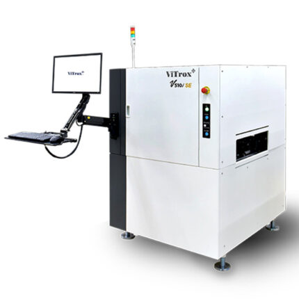
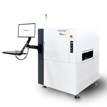

V810i S3 ViTrox | Advanced 3D X-Ray Inspection system (AXI)
V810i S3 ViTrox | X-Ray
- Various Platform to cater different board sizes
- Worldwide support coverage
- High Speed Inspection
ViTrox X-Ray Inspection System
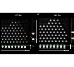
New Reconstruction Method for CT Technologies – Algebraic Reconstruction Technique (ART)
Provide alternative view (3D model) for defects buy off and increase user confidence to buy off defect. At the same time, it will generate defect failure analysis for further improvement.
Alternative view (3D model) for defects buyoff
Increase users confident to buyoff defects
Defect failure analysis
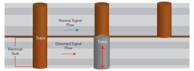
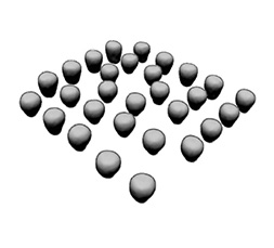
A typical through hole VIA without backdrill results in reflections, capacitance, & inductance discontinuities which will degrade the signal integrity
Backdrill the unused stub with a controlled depth
After backdrill, the signal will not flow to unwanted stub and minimize signal integrity degradation
| Model.No | V810i S3 |
| System controller | Integrated controller with 8 Core Intel Xeon processors |
| Operating system | Windows 10 (64 bits) |
| User interface | Microsoft Windows based software solution with easy-to-use GUI and password-protected user levels |
| Off-line test development software | Optional for off-line PC |
| CAD conversion tool | Support 4 different types of CAD in V810i software and optional software available to translate other CAD data to ViTrox’s format |
| Typical test development time | 4 hours to 1.5 days to convert raw CAD file and develop application |
| Transport heights | 865mm-1025mm |
| Line communication standard | SMEMA, HERMES |
| Barcode readers | Compatible with most industry standard barcode readers |
| Typical image acquisition rate | 51.68cm²/sec (8 in²/sec) at 19µm |
| False Call rate | 500-1000ppm |
| Joint pitch1 | 0.3mm and above |
| Short width2 | 0.045mm |
| Solder thickness | 0.0127mm |
| Power Supplies | 200–240 VAC three phase; 380–415 VAC three phase wye (+/- 5) (50Hz or 60Hz) |
| Air requirement | 552kPA (80psi) compressed air |
| System footprint (Width X Depth X Height) | 1835mmx2185mmx2162mm |
| Total system weight | ~4000kgs |
| Maximum PCB Size (L x W) | 725mmx482.6mm (28.5″x19″) |
| Minimum PCB Size (L x W) | 63.5mmx63.5mm (2.5″x 2.5″) |
| Maximum PCB inspectable area | 725mmx474.9mm (28.5″x18.7″) |
| Maximum PCB thickness | 7mm (276 mils) |
| Minimum PCB thickness | 0.5mm (20 mils) |
| PCB warp | Downside < 3.3mm; Upside < 3.3mm |
| Maximum PCB weight | 4.5kg |
| Top Clearance of PCB | 50mm * 22μm resolution 44mm * 19μm resolution 28mm * 15μm resolution 13mm * 12μm resolution 28mm * 10μm resolution 13mm * 7μm resolution (calculated from board top surface) |
| Bottom Clearance of PCB | 80mm |
| PCB edge clearance | 3mm |
| 100% Press-fit testability | Yes (With PSP2 / PSP2.1 feature) |
| PCB Temperature | 40 Deg C |


Reviews
There are no reviews yet.